If you have been following my recent progress with the AIS-gPPT3-1C Propulsion Module, you will have seen that during the recent impulse-bit test, at shot #130 for the thruster, the thruster stopped working. Taking it out of the vacuum chamber and troubleshooting the board, my primary suspicion was confirmed – the main capacitor bank had failed, shorting internally causing the high voltage supply to short through the capacitor, ceasing thruster operation. Since the capacitors I originally selected were standard high voltage SMT non-pulse rated capacitors using standard X74 dielectric, I knew this would eventually be an issue. However, I was quite surprised that the main cap bank failed so rapidly.
Fortunately, this is not the end of the world, and a great chance in fact to upgrade the system. There are high performance SMT pulse capacitors you can buy off the shelf, though unfortunately they are quite pricey and much larger form factor. Therefore, the board design would have to be reworked to accommodate these new capacitors.
I ended up selecting the KEMET MLCC high-voltage pulse-rated SMT capacitors. These capacitors boast impressive performance – at around 1kV charging voltage, they can deliver around 1kA of pulsed current! These capacitors are state-of-the-art designed for harsh environment conditions and pulse detonation applications. They are on the pricey side however – depending on operating voltage and capacitance, they can range from around $30 per cap to $60. They are also on the larger side, with a custom SMT size of 4540, measuring at nearly 0.5″ square at 0.1″ thickness! Fortunately however, despite my extremely limited space, I managed to rework the board design to accommodate these new capacitors.
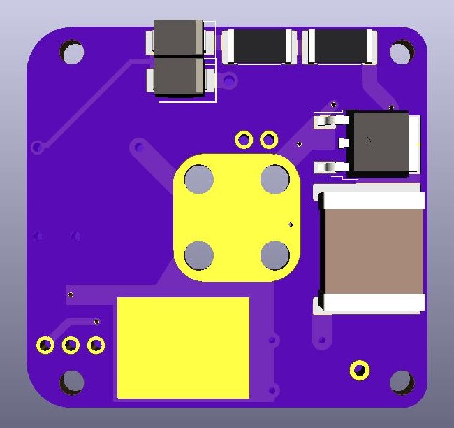
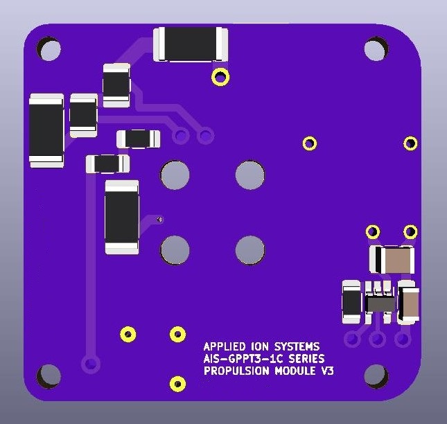
Below are the KiCad renders of the newest V3 iteration of the PCB electronics board for the thruster. Although the standard cap for the igniter bank was still perfectly fine and in working order, I figured it would be best to not take any risks and just upgrade that capacitor as well. The capacitor can actually be seen in the first render below as the large square cap on the right side of the board. I also increased the main bank soldering area to fit these new capacitors, which is the large exposed pad at the bottom of the board in the first render. This should be enough space to accommodate up to 3 capacitors in parallel when vertically soldered. Due to voltage and capacitance rating availability of these caps, I opted to go with the 1kV nominal (2kV max) rated 0.068uF versions. Using three of these in parallel brings me right to the regular bank capacitance of the prior version at 0.2uF. In order to fit both upgraded cap banks, I moved all of the voltage measurement circuitry to the back. Now, all of the high voltage and pulse circuitry is located on the top layer of the board, and all of the control and measurement circuitry is located on the back layer of the board.
Now, here comes the interesting optimization part. I do have the option of reducing the bank energy by using less capacitors in the main bank. If I go with two of the 0.068uF caps in parallel, this makes the total capacitance now 0.136uF, bringing total energy down further to 0.06J. What would be the benefit of doing this besides some cost reduction? With this lower capacity, nominal rep rate can be increased to 0.5Hz. At this level, with 60% supply efficiency, peak input power requirements drops to 550mW from 850mW, with an average input power dropping further to 113mW from 163mW over the charging period. So we can charge the bank faster with less power, which is to be expected from this change.
Now, let’s look at performance. If we assume the scaling for this thruster holds at roughly I-bit=0.6744e^(1.2923*energy) (established from prior I-bit testing), correcting for the new thruster performance difference, at 0.06J I can still reasonably expect ~0.63uNs impulse-bit. This is down a negligible amount from the already estimated 0.65uNs impulse-bit performance at 0.09J. Now here is where things get interesting! Although impulse-bit is lower, at the increased rep rate of 0.5Hz, thrust is now 0.32uN, which is up by 69% over current performance of 0.22uN! With an optimized thruster design, by reducing energy per shot, resulting in higher rep rate, thrust actually increases with lower power! Even if we assume a radical drop in impulse-bit to 0.5uNs, thrust is still 0.25uN, which is still slightly higher than the current thrust level at higher bank energy at lower rep rate, while still reducing total power consumption by a decent amount. Further bank capacity reduction could still increase thrust even more as rep rate increases, leading to an interesting optimization trade-off for performance.
The new V3 board design is currently in the process of being manufactured, and should actually arrive in the next few days. I am hoping this will be the first flight versions, which I will be soldering, testing, and actually delivering to Fossa Systems for our joint mission collaboration. I will also be looking to do some of the first ever live-streaming of the upcoming qualifying lifetime tests for this new flight module in preparation for the Fossa Systems mission. Lots of exciting things to come in the next couple of weeks!